Project Info
The iTPM ADFE (italian Tile Processor Module Analog to Digital Front-End) is responsible for Analog to Digital conversion and pre-processing of 32 analog inputs with sampling frequencies from 700 MHz up to 1 GHz.
Description
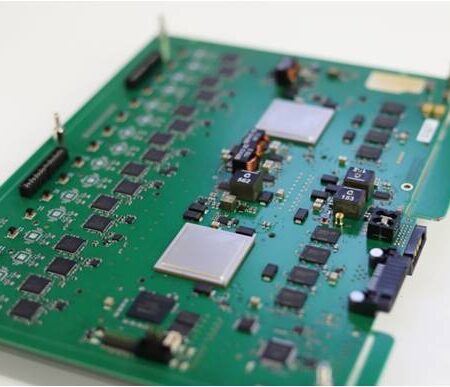
The iTPM ADFE (italian Tile Processor Module Analog to Digital Front-End) is responsible for Analog to Digital conversion and pre-processing of a multi-channel source, managing up to 32 analog inputs with sampling frequencies from 700MHz up to 1GHz. Two acquisition modes are available: 32 8-bit channels and 16 14-bit channels. Best in class 14 bit AD converter, recent 20nm FPGA, 40Gbit Ethernet optical link have been selected focusing on the best commercial compromise between quality, performance and power consumption. Compact board size, low noise clock network, advanced 14-layer board build-up, Ethernet based management features (including health monitoring capability), high efficiency and low noise power distribution system complete the main board features. Accurate board design allow an High Density RF interface with superior performances with high linearity, low interference between channels to meet really challenging requirements. The board has been developed in collaboration with INAF and Oxford University in the frame of the Square Kilometer Array (SKA) international project, and is used within the antenna receiver module of the radio telescope. The beamforming technique is successfully adopted in the directional signal reception, thanks to this powerful board.
Key Features
- 32 RF input @ 1 Gsps, 50 Ohm
- Analog Devices AD9680, 14 bit high performance ADC
- Digital beamforming
- 50 MHz – 650 MHz analog band
- Channel isolation > 60 dB
- ENOB > 7.89
- JESD204B Subclass 1, 2×16 lines
- 2x XILINX UltraScale XCU40 FPGAs
- Open FPGA
- Compact size, 6U format compatible
- 2x 40G Ethernet interfaces
- 2x 80 bit DDR3L @ 1.6 Gbps
- Management instant ON Lattice CPLD with Ethernet Gigabit Link
- System Monitor
- 256Mbit SPI on board FLASH for multiple FPGA configuration
- High efficient Power Distribution System, single input DC supply
- EMI verified
- 105 Watt load with test application
Board Technical Specifications and Characteristics
Thanks to the JESD204B interface all the ADs are source synchronous and can be phase aligned with a 10 MHz external reference and PPS. Two identical FPGAs interface eight dual channel ADs with 16 JESD204B 10GBps lines, 80 bit DDR3L memory and a 40G Ethernet interface with a QSFP+ connector. A management CPLD is present with a dedicated Ethernet Gigabit link for loading firmware and monitoring temperature and voltage over 40 internal points .

| Component Description | Component |
| Management CPLD | Lattice Semiconductor LCMXO2-7000HC |
| Management FLASH | 512 Mbit SPI |
| FPGA | 2x Xilinx XCKU040-2FFVA1156E |
| FPGA Memory | 1512 MByte DDR3L @1.6 Gbps |
| Analog to Digital Converter | Analog Devices AD9680 |
| Front Panel Connectors | 2x QSFP |
| SMA, external 10Mhz reference | |
| SMA, PPS | |
| Input Supply | |
| RJ45 Gigabit | |
| RF INPUT Connectors & GPIO | 4x ISORATE IP5 08 |
| 2x ERF8 010 | |
| Internal GPIO | 2 x 2 GPIO |
| Debug Connector | FPGA JTAG |
| Power Supply | 12-24 VDC |
| Power Consumption | Up to 150W |
| Working Temperature | +5°C / +55°C |
| Board size | 23 mm x 170mm x 31mm |
RF Qualification Results
The RF performances and the compete set of digital functions of each production board have been extensively verified by INAF. Relevant results obtained with the RF qualification are provided in the pictures below. The measurements are provided acquiring data on 32 8-bit channels, in two board configurations, with and without ADA devices; two bandwidths are investigated, 50-375MHz and 375-650MHz, running at sampling rate 800MHz and 700MHz respectively.


Remarkable Figures Measured during the Qualification Process
| Fs: 800 MSPS -– BW: 50 – 375 MHz | ||
|---|---|---|
| ADC Performance Parameters | ADU Board#1 (with ADA) | ADU Board#2 (without ADA) |
| Signal to Noise Ratio referenced to Full Scale [dBFS] | ≥ 49.19 | ≥ 49.33 |
| Gain Flatness [dBFS] | ≤ ±0.3573 | ≤ ±0.343 |
| 2nd-order Harmonic Distortion [dBc] | ≤ -67.24 | ≤ -67.74 |
| 3rd-order Harmonic Distortion [dBc] | ≤ -66.53 | ≤ -68.56 |
| Worst Other Spur [dBc] | ≤ -67.03 | ≤ -66.83 |
| Spurious Free Dynamic Range [dBc] | ≥ 66.53 | ≥ 66.83 |
| ENOB [bits] | ≥ 7.876 | ≥ 7.896 |
| Cross-Talk [dBc] | ≤ -65.69 | ≤ -61 |
| IP3 [dB] (F1=184.7 MHz; F2=187.5 MHz) | 1,246527778 | 32.2 |
| IP2 [dB] (F1=184.7 MHz; F2=187.5 MHz) | 66.3 | 77.5 |
| Fs: 700 MSPS — BW: 375 – 650 MHz | ||
| ADC Performance Parameters | ADU Board#1 (with ADA) | ADU Board#2 (without ADA) |
| Signal to Noise Ratio referenced to Full Scale [dBFS] | ≥ 48.88 | ≥ 49.32 |
| Gain Flatness [dBFS] | ≤ ±0.6252 | ≤ ±1.356 |
| 2nd-order Harmonic Distortion [dBc] | ≤ -65.77 | ≤ -59.9 |
| 3rd-order Harmonic Distortion [dBc] | ≤ -60.78 | ≤ -65.64 |
| Worst Other Spur [dBc] | ≤ -64.16 | ≤ -63.23 |
| Spurious Free Dynamic Range [dBc] | ≥ 60.78 | ≥ 59.9 |
| ENOB [bits] | ≥ 7.788 | ≥ 7.886 |
| Cross-Talk [dBc] | ≤ -70.58 | ≤ -70.39 |
| IP3 [dB] (F1=500.1 MHz; F2=503.2 MHz) | 26 | 24.4 |
| IP2 [dB] (F1=500.1 MHz; F2=503.2 MHz) | 64 | 58.3 |
Sanitas EG reserves the right to change specifications without notice