Project Info
The HP-DDR2 Controller is a high-performance, special-purpose memory controller that interfaces with industry standard DDR2 memory devices (667/533/400/333/266 MHz) and provides a common command interface for user applications.
Description
This core is aimed at optimizing both performances and resource usage. The controller adapts the execution of memory access commands in order to exactly match the timing requirements imposed by the parameters. The memory controller supports burst memory read and write accesses with dynamic burst size, and manages memory initialization and refresh cycles. The very small DDR2 state machine controller, characterized by a few levels of logic, allows for very high operating frequencies.
| Resource Utilization Lattice XP2™ 32-bit interface |
|||
|---|---|---|---|
| SLICE | LUT | Register | Fmax(MHz) |
| 385 | 280 | 680 | 333 (667 DDR) |
Key features
- High Performance DDR2 667/533/400/333/266 operations (tested on Lattice XP2™ LFXP2-17E-5 devices)
- Interfaces to industry standard DDR2 SDRAM devices and modules
- Multiple SO/DIMM support
- Supports unbuffered DIMM
- SDRAM data path widths of 8, 16, 32, 64 and 72 bits
- Variable address widths for different memory devices
- CAS latency of 3, 4, 5 or 6 cycles (via VHDL generics)
- Command burst capability with dynamic burst size control
- Programmable memory timing parameters via VHDL generics
- Byte-level writing through data mask signals
- Automatic Auto_refresh management
Technical Description
The finite state machine controller is very compact and allows for an extremely optimized implementation, and high operational frequency . Nevertheless, it manages the initialization and the auto-refresh.
For each user command the sequence active, read/write, and precharge is performed by the controller . The bank management is not implemented. This saves logic resources, allows reaching high frequencies, makes the real performance evaluation independent from the user application, and achieves the minimum latency for concurrent accesses spread across the whole memory, typical of multiport applications.
Latency can be computed according to the following formula:
Read Latency = tRCD + cas_latency + 10
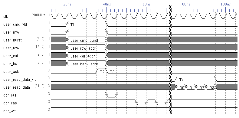
Where tRCD is the delay between ACTIVATE and READ or WRITE commands and cas_latency is selected CAS latency . The Read Latency is expressed in clock cycles and represents the time period between T1 and T4 events.
Read and Write Operations
The HP-DDR2 Controller provides a common user interface. Waveforms below show the read operation.
Verification
The IP core has been tested using the demo board XP2 Advance Evaluation, hosting a Lattice LFXP2-17E-5 device. The core has been tested up to 333 MHz and it compiles also at 400 MHz.
Optional modules
Two optional modules are available: Multiport Controller and Wishbone Interface.